Develop a new design
The frequency plan, available space, interfaces and performance targets form the basis for the concept, simulation, circuit, layout and prototype.
SERVICES
New designs, optimisation or product customisation: we handle the technical work along your entire RF signal path.
WORKING TOGETHER
The frequency plan, available space, interfaces and performance targets form the basis for the concept, simulation, circuit, layout and prototype.
We measure current performance, identify the limiting factor and make targeted changes to the antenna, matching, layout or integration.
We review our product range and adapt tuning, connectors, cables or mechanical design to your device.
SYSTEM APPROACH
The order and combination of components depend on the transmit and receive paths. We consider impedance, loss, noise and coupling at every interface.
THE COMPLETE RF PATH
From the antenna element through filters, LNAs and cables to impedance control on the PCB and the RF chip: we develop, optimise and measure the entire connection.
01 / From embedded antennas to antenna arrays
We develop passive and active antennas for the actual installation. The PCB, enclosure, ground plane, mounting and proximity to the user are included in the electromagnetic design.
Your deliverablesAntenna geometry, integration recommendations, matching network and documented simulation and measurement results.
02 / Signal quality in the front end
We design RF assemblies for the required signal levels, frequency plan and interference environment. In the receive path, we consider gain and noise figure together with losses ahead of the first amplifier.
Your deliverablesCircuit diagram, component selection, RF layout, prototypes and agreed measurement data for the assembly.
03 / From the antenna connector to the RF chip
We review and optimise the complete RF path on the PCB. A nominally 50 Ω trace alone does not guarantee a low-loss transition between components, layers and connectors.
Your deliverablesAn annotated layout review with prioritised changes, or an agreed redesign including simulation of critical transitions.
04 / Decisions before the first prototype
We translate frequency bands, geometry and performance targets into a simulation model. Comparisons show which antenna position, feed arrangement or enclosure modification is technically appropriate.
Your deliverablesFeasibility assessment, comparison of alternatives and design recommendations with clearly defined technical constraints.
05 / Validating simulation in the installed product
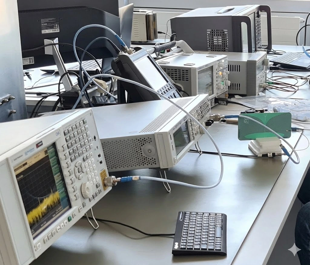
We characterise antennas and RF assemblies and investigate inadequate range or reception quality. Measurements distinguish mismatch, transmission losses, interference coupling and shadowing.
Your deliverablesA measurement report covering the setup, conditions, findings and specific optimisation measures. Regulatory testing is agreed as a separate scope.
06 / Developing electronics and mechanics together
We develop radio PCBs and integrate antennas into existing electronics. In compact devices, we treat power supplies, digital interference sources, battery, enclosure and antenna as one system.
Your deliverablesFunctional prototypes, circuit and layout documentation, integration guidance and measurement data for the next development decision.
07 / Fields, coupling and shielding
We also work beyond conventional radio modules: waveguides, resonators, high-power microwave assemblies and inductive power transfer. Our experience ranges from implant charging systems to industrial microwave applications.
Your deliverablesField analysis and design measures tailored to power, frequency, installation environment and the agreed test objective.
08 / From a standard product to a customised variant
We first assess whether an existing antenna, filter, LNA or cable assembly meets your requirements. If necessary, we customise the product or develop a new version and can take responsibility for mass production.
Your deliverablesAn approved product version with agreed electrical, mechanical and quality requirements.
PROJECT WORKFLOW
We agree performance targets, deliverables and test conditions. Concept development and simulation are followed by circuit and layout design, prototyping and measurements in the intended installation. Deviations are addressed through documented iterations.
For series production, we agree manufacturing data, tolerances, test equipment and quality criteria. Confidentiality, usage rights and development scope are defined for each project. Individual layout reviews, feasibility studies and measurement tasks are also available.
WORKFLOW
We define frequencies, available space and performance targets, assess alternatives through simulation and measure prototypes in the device.
Technical services →PRODUCTS
Antennas, low-noise amplifiers, RF filters and micro-coaxial cables: we select existing parts, customise them or develop a new solution including the PCB RF path.
CA-MHF4-MC1.13-075-MHF4
up to 6 GHz
PROJECTS
Explore selected development tasks and the technical steps we use to address them.
Automotive radar
Identification and tracking
High-speed data lines
YOUR REQUIREMENTS
Frequency bands, available space, enclosure and performance targets are our starting point.